Very Large Scale Integration (VLSI)
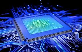
Very-large-scale integration (VLSI) is the process of creating an integrated circuit (IC) by combining thousands of transistors into a single chip. VLSI began in the 1970s when complex semiconductor and communication technologies were being developed. The microprocessor is a VLSI device. Before the introduction of VLSI technology most ICs had a limited set of functions they could perform. An electronic circuit might consist of a CPU, ROM, RAM and other glue logic. VLSI lets IC designers add all of these into one chip.
DEVELOPMENTS
The first semiconductor chips held two transistors each. Subsequent advances added more transistors, and as a consequence, more individual functions or systems were integrated over time. The first integrated circuits held only a few devices, perhaps as many as ten diodes, transistors, resistors and capacitors, making it possible to fabricate one or more logic gates on a single device.
DEALING WITH VLSI CIRCUITS
Digital VLSI circuits are predominantly CMOS based. The way normal blocks like latches and gates are implemented is different from what students have seen so far, but the behaviour remains the same. All the miniaturisation involves new things to consider. A lot of thought has to go into actual implementations as well as design. Let us look at some of the factors involved
1. Circuit Delays
Large complicated circuits running at very high frequencies have one big problem to tackle - the problem of delays in propagation of signals through gates and wires ... even for areas a few micrometers across! The operation speed is so large that as the delays add up, they can actually become comparable to the clock speeds.
2. Power
Another effect of high operation frequencies is increased consumption of power. This has two-fold effect - devices consume batteries faster, and heat dissipation increases. Coupled with the fact that surface areas have decreased, heat poses a major threat to the stability of the circuit itself.
3. Layout
Laying out the circuit components is task common to all branches of electronics. Whats so special in our case is that there are many possible ways to do this; there can be multiple layers of different materials on the same silicon, there can be different arrangements of the smaller parts for the same component and so on.
THE VLSI DESIGN PROCESS
A typical digital design flow is as follows:
Specification
Architecture
RTL Coding
RTL Verification
Synthesis
Backend
Tape Out to Foundry to get end product….a wafer with repeated number of identical Ics.
All modern digital designs start with a designer writing a hardware description of the IC (using HDL or Hardware Description Language) in Verilog / VHDL. A Verilog or VHDL program essentially describes the hardware (logic gates, Flip-Flops, counters etc) and the interconnect of the circuit blocks and the functionality. Various CAD tools are available to synthesize a circuit based on the HDL. The most widely used synthesis tools come from two CAD companies. Synposys and Cadence.
Without going into details, we can say that the VHDL, can be called as the "C" of the VLSI industry. VHDL stands for "VHSIC Hardware Definition Language", where VHSIC stands for "Very High Speed Integrated Circuit". This language is used to design the circuits at a high-level, in two ways. It can either be a behavioral description, which describes what the circuit is supposed to do, or a structural description, which describes what the circuit is made of. There are other languages for describing circuits, such as Verilog, which work in a similar fashion.
A typical analog design flow is as follows:
Specifications
Architecture
Circuit Design
SPICE Simulation
Layout
Parametric Extraction / Back Annotation
Final Design
Tape Out to foundry.
Language : VERILOG, VHDL
Design tools : MODELSIM, XILINX, MICROWIND, TANNER, Cadence, Synopsys


